AM-Stereo M-CQUAM Modulator
AM-Stereo M-CQUAM Modulator

As a European collector of vintage radios, in the past I have always accepted the fact that AM is broadcast in mono. It was only recently that I discovered that in the US and other countries AM stereo broadcasts exist to this day. I was immediately interested in the technology behind AM stereo broadcasting. More or less by coincidence I stumbled across the document that Dietmar Rudolph had posted in this forum. I also found Robert Weaver's AM Stereo Tube transmitter. Both posts have been extremely helpful in understanding the inner workings of AM stereo and were the basis that enabled me to build my projects. I have two designs that I will introduce in this forum. One utilizes Russian tubes mostly and the other uses vintage integrated circuits. I will start with the latter in this thread.
Since I have relatives in the US it was easy for me to gain access to some AM stereo equipment. I own a Sony SRF-A100, SRF-A1, SRF-A10 and a JC Penney MCS3050. A Carver TX11a will find its way to Germany in a few months as well, I hope...
After a few weeks of experimenting I decided to build a modulator that works according to the M-CQUAM system described in the document by Dietmar Rudolph above. For test purposes I had built both a regular CQUAM modulator and an M-CQUAM modulator and had tested both with the receiving equipment I have. With the equipment at hand I could not find any difference in terms of channel separation or audio fidelity between the two versions; therefore, I decided to go for the M-CQUAM design for my semiconductor version of the modulator.
I will start with some theory first. A regular CQUAM modulator contains a Quadrature Amplitude Modulator where the I axis is modulated by the L+R signal and the Q axis is modulated by the L-R signal. Additionally in the I section a +1 offset is added so the carrier is present at all times. The resulting signal is then passed through a limiter that strips the signal of its amplitude modulation leaving only a phase modulated signal with a fixed amplitude.
An M-CQUAM modulator is a simplified version of the above where the I axis part has been replaced by a simple fixed carrier adder network. This results in only the L-R signal modulating the Q axis carrier portion. The I portion is fixed. After passing the limiter the resulting signal once again only contains the phase modulation part.
The phase modulated carrier then is passed through an envelope modulator and is AM modulated by the L+R signal.

Here you can see a vector representation of the L-R modulation in the M-CQUAM process. The tip of the resulting vector traces a straight line and has a maximum phase deviation of +/-45°. This is the situation before the signal is passed through the limiter.
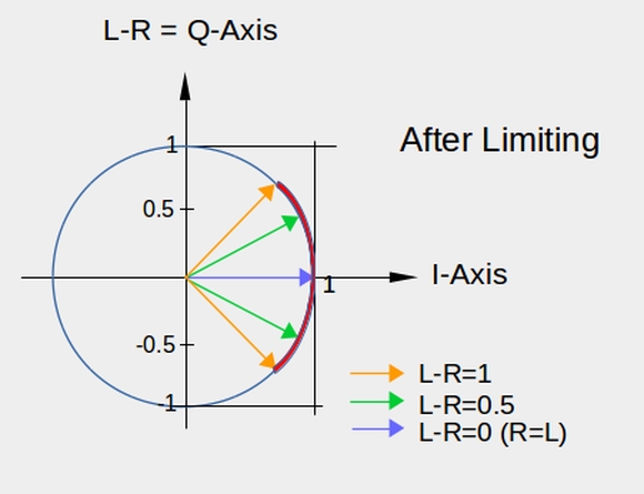
After passing through the limiter the signal amplitude is fixed. The resulting vector now traces a circular curve shown in red here but exhibits the same phase deviation as before.The following block diagram illustrates the signal processing of the M-CQUAM modulator I have designed: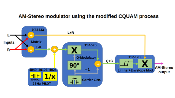
It consists of the following parts:
- Stereo matrix to generate the L+R and L-R signals
- Carrier oscillator and Q axis modulator
- Adder network to merge I and Q axis signals
- Limiter for the QAM signal
- Envelope modulator for the L+R signal
- 25Hz pilot generator
- Output stage
The circuit diagram can be found in the attachment. I will proceed in describing the individual building blocks of my modulator.
Stereo matrix:
This was built with the NE5532 low noise operational amplifier.
.png)
U1A and U1B form a buffer for the L and R signals input via P1. The buffered signals are then fed to the matrix IC U2. U2A forms the L+R signal and U2B delivers the L-R signal. The L-R signal level can be adjusted by RV3. It should be set for best channel separation.
Increasing the L-R level beyond the point of maximum channel separation will yield a „super stereo“ effect.
Resistors R15-21 should be 1% types to achieve an accurate matrix function. Header P3 is intended for a level indicator and carries the L+R/L-R signals as well as a 12V supply for a level indicator board. In order to avoid over modulation only the L+R signal actually needs to be monitored as this is fed to the envelope AM modulator which should not be driven beyond 70-80% modulation.
Carrier Oscillator and Q-Axis Modulator:
The carrier can be generated internally with a crystal or ceramic resonator as the frequency determining item. There is also a provision via P5 to feed an externally generated carrier signal into the board.
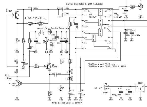
The modulator U3 utilizes a PAL color decoder IC as an oscillator and Q axis modulator. The board is designed to work with either the TBA520 or the later TBA990 ICs.
A PAL decoder consists of two balanced modulator (Gilbert) cells that act as the R-Y and B-Y demodulators respectively and a color matrix to form the G-Y color signal. The latter is actually an adder network that adds the two demodulated signals according to the following formula:
0.51x(R-Y) + 0.19x(B-Y)
In this design I used the G-Y adder network to add the I axis carrier and the dual sideband (DSB) modulated L-R signal togehter, thus forming a QAM signal. The „R-Y“ signal in this case is the I axis oscillator, i.e. carrier signal, and „B-Y“ is the 90° shifted Q axis signal modulated by the L-R audio signal from the audio matrix. The resulting QAM signal in conveniently available at Pin #5 of U3.
The R-Y channel forms the oscillator with amplitude regulation. This ensures a fixed carrier amplitude that should be adjusted to 300mVpp @MP1 by RV2. The R-Y balanced modulator is used as a voltage controlled amplifier (VCA). Its output available at pin #4 is fed to Q2 and Q3 which act as buffers. After passing Q2 the oscillator signal goes through crystal Y1 and then to the input of the R-Y demodulator, thus closing the feedback loop needed for oscillation.
Q3 feeds rectifier diodes D1 and D2 which generate a voltage proportional to the oscillator amplitude. This control voltage is available at C15 and is fed to the R-Y modulator via pin #2, thus controlling the amplification of the oscillator circuit.
Part of the ocillator signal buffered by Q2 is fed to Q1 which together with R7, RV1 and C5 forms an adjustable phase shifter. RV1 needs to be set for an exact 90° phase shift at the carrier frequency @MP3. There is an easy method to verify this as I will decribe in a separate „adjustment and setup“ part. The values given in the circuit diagram will work for freqencies around 1400kHz; for lower frequencies C5 should be increased to 220p or more. The 90° shifted carrier is fed to pin #9 if U3 is a TBA520 or to pin #10 if U3 is a TBA990. In both cases this is one input of the B-Y balanced modulator.
The L-R audio signal is fed to the other input of the B-Y balanced modulator inside U3 via pin #8. The modulation is a DSB with suppressed carrier. Carrier suppression can be optimized with RV4. This should be adjusted for minimal carrier output @MP3 with no L-R signal and the pilot switched off.
The resulting DSB modulated L-R signal is mixed with the the 0° I axis carrier in the box „G-Y Mat“ in U3. The resulting QAM signal is output via pin #5 and can be monitored @MP5.
Limiter and Envelope Modulator:
The QAM signal generated by U3 is now fed to a TBA120 (SN76660) IC. This is actually an FM demodulator for TV sets, but due to the fact that it contains both a limiter and a balanced modulator it is ideal for the task of generating the final M-CQUAM signal.
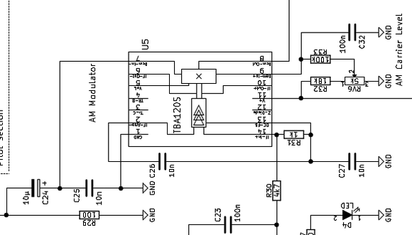
The QAM signal is fed to U5 pin #14 via R30. Inside U5 the signal is amplitude limited and passed to the internal balanced modulator. This balanced modulator acts as the envelope AM modulator. The L+R signal from the matrix is fed to this modulator via U5 pin #7. In order to achieve a regular AM modulation with carrier, an offset is added to the balanced modulator with R33 and RV6. RV6 sets the 50% carrier level with no L+R signal.
The M-CQUAM modulated output signal is available at pin #8. Since the internal limiter of U5 generates a square wave signal with many harmonics, the output needs to be low-pass filtered to achieve a clean signal free of harmonics. This is done in the output buffer section.
Output Stage:
In order to provide a low impedance output that can drive a 50Ω coaxial cable e.g. RG58, an output buffer was implemented using the LT1227 chip. This IC can drive low impedance loads and delivers up to 4Vpp into a 50Ω cable.
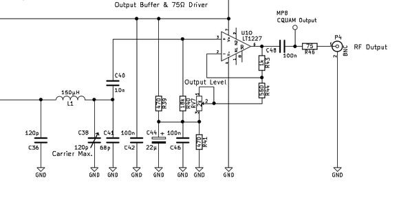
C36, L1, C38 and C41 form a low-pass filter that supresses harmonics in the signal output of U5. C38 should be adjusted for maximum signal amplitude. It should exhibit a clear peak in the signal level in a mid-range position i.e. not at the minimum or maximum value. If this cannot be achieved C36, L1 and C41 need to be changed to match the desired frequency of operation. The values given are suitable for freqencies around 1400kHz. The circuit can drive either a 50Ω or a 75Ω load. Resistor R40 needs to match the desired load impedance.
25Hz Pilot Generator:
The Motorola CQUAM AM stereo system uses a 25Hz pilot modulated on the Q axis carrier to allow receivers to automatically identify stereo broadcasts. In this modulator I used a 400kHz ceramic resonator with some digital dividers to generate this signal.
In order to generate a 25Hz signal from a 400kHz oscillator, the signal frequency has to be divided by 16000 since 400,000/25=16000. If we perform a prime factorization on this number, it yields the integers of:
2,2,2,2,2,2,2,5,5,5
The high number of 2s is an advantage here since a division by two can be handled by many CMOS dividers like the 4040, 4060 or 4024. The three 5s can be handled by a programmable divider. In this case I used the programmable CMOS binary down counter 40103. So the whole division process can be performed by first dividing the 400kHz signal in the following manner:
Step 1: 5x5x5x2=250 done by U7 a CMOS 40103 programmed to the value of „250“
followed by
Step 2: 2x2x2x2x2x2=64 done with U9 a 4024 using the (Q7) output
64x250=16000 which is the desired division factor.
I started with the „250“ factor so I could place the binary counters at the end of the divider chain giving me a 25 Hz square wave with a 50% duty cycle that would nicely filter into a sine wave. The output of the 40103 is a short pulse of a few micro seconds which would have been much more difficult to strip of its harmonics.
To allow more flexibility in choosing resonators I included jumpers that allow the selection of either the Q7 or Q8 output of U9. This measure allows the use of an 800kHz resonator when Q8 is selected. For a 400kHz one Q7 has to be selected.
The resulting signal is a square wave so it has to be passed through a low pass filter to become a clean sinsoidal waveform. Since I needed a CMOS 4049 to act as an oscillator for the 400 kHz resonator anyway, I decided to use most of the remaining gates in that IC in linear mode for the low-pass filters. After passing through low-pass filters the pilot has a nice sinsoidal shape with an amplitude of around 1Vpp at R47.
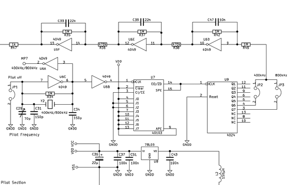
The pilot level can be set with RV5. I ususally increase the level until the „Stereo“ indicator on my receivers turns on and then increase the level slightly from that point.
Conclusion:
The project was built on a printed circuit board measuring 100x150mm. Here is an image of one of my boards.

I have four of them running in my house 24/7 delivering signals to my collection of vintage radios and receivers. Since CQUAM is compatible with old radios that employ envelope detectors I can use these signals with all of my radios.
The project data for the PCB is available in KiCAD. Please email me if you are interested in a copy for non commercial use.
Attachments:
- M-CQuam_odulator_Circuit Diagram (177 KB)
To thank the Author because you find the post helpful or well done.