panasonic: RF-869JB RF troubleshooting
panasonic: RF-869JB RF troubleshooting

Got one of these nice radios; it was sold as a collectible item, so I assumed it would be defective.
Indeed it was dead on arrival. By putting my ear to the speaker, I could hear a very slight background noise typical of an audio amplifier.
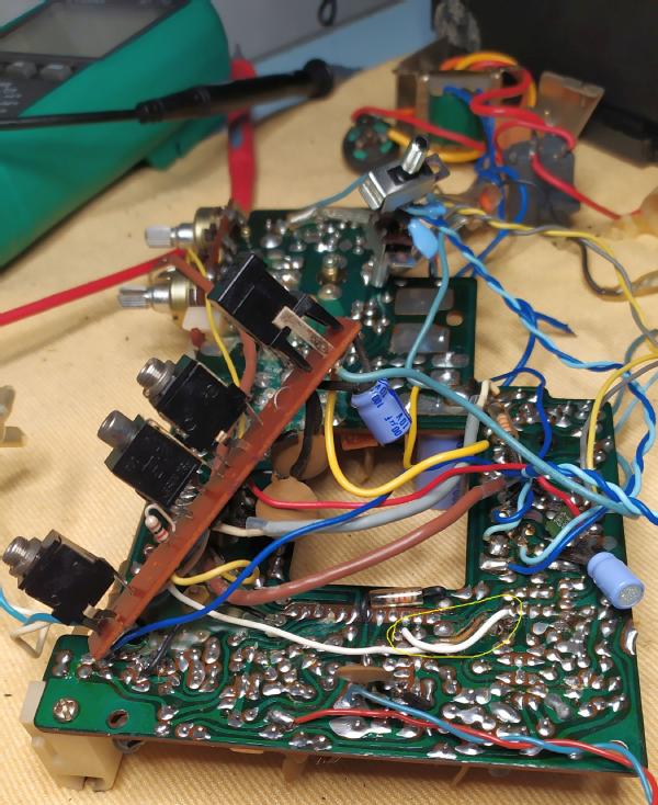
The battery compartment looked clean. However after removing the long screws that keeps the front, rear, and middle plastic parts together as a sandwich, some greenish residues of battery leakage were visible on the battery terminals that are hidden when the radio is assembled.
As it is almost impossible to service this radio without removing the PCB assembly from the main chassis frame that hides part of the PCB copper traces side, I spent around an hour dismantling the switches, dial scale, jacks, unsoldering a few wires of the BATT CHECK press button and some power lines.
A quick visual inspection did not revealed any corrosion on the PCB or components.
The audio section was fully working, as touching the volume potentiometer with a screwdriver resulted in a strong 50Hz noise from the speakers.
However, all the three RF bands were absolutely silent. No noise coming from the IF section. Also the nice PMMC analog meter looked to be dead, despite being in good shape (R=630 Ohm).
As I am away from my usual home and have no access to a proper signal generator, I used a portable oscilloscope to check for RF noise at the last IF section. Nothing.
A brief checking of the power supply voltages at the three IF transistor stages told me that around 4.3V was present.
As I could not find a schematic diagram anywhere, I started doing some reverse engineering and drawed the audio section and part of the IF sections.
As usual on similar National Panasonic models of that era, the power supply positive pole goes to a virtual ground (distinct from the RF ground) , while the negative pole acts as a common reference level.
NPN transistors are used in this model (except for one 2SA683 PNP at the complementary audio output stage).
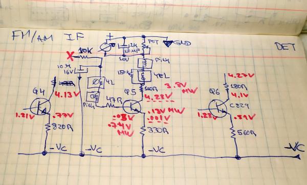
The three IF stages are setup in common emitter mode, where the emitter goes to the negative power supply line (-Vc) thru a series resistor, while the collector goes to the positive line (+Vc) close to the RF ground thru two IF transformers and a resistor in series.
For all intents and purposes, I assumed the -Vc line as the common reference point for voltage readings.
The obvious suspect IF stage was the middle one, where the PMMC meter is inserted at the collector side in series with the two IF transformers and a 100R resisstor. The PMMC have a parallel 5KR trimmer to adjust its full scale position. The 2SC829 emitter have a 330R to -Vc.
Indeed the base terminal of the 2SC829 was at 0.05VDC, the emitter at 0.001VDC, and collector at 4.28VDC. So the transistor was basically in cut off state.
By following the transistor base terminal connections, a series of a 47R resistor and two IF transformers looked good. An 10uF 16V electrolytic capacitor should filter a voltage coming thru a series 10KR resistor feeding the above series transformers. However, no voltage was preesent at this joint.
The good old continuity check revealed the issue. The copper trace was interrupted at one side of the 10KR resistor. Although the copper traces looked visually perfect as they are painted with green varnish. Only after scratching the varnish I could see the copper totally oxidized from the battery electrolytes.
After using a wire to bypass the faulty copper trace, the 2SC829 base now have 0.74VDC, the emitter 0.13VDC, and the collector 3.8VDC (MW band).
And yes, the radio came to life again, on all three bands.
Meanwhile I found a seller on Rakuten offering a set of Panasonic RF series service manuals, so I ordered them two days ago and waiting for shipment. I will upload the schemaatics as soon as I get the goods.
PCB assy ready to be removed from the middle section chassis frame:

PCB assy free from the frame and ready for troubleshooting:

And the faulty copper trace bypassed with a white wire.:
My schematic drafts. Very incomplete and a few errors, be aware. PCB components layout:
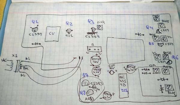
Audio section:
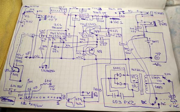
RF IF section:
To thank the Author because you find the post helpful or well done.
panasonic: RF-869JB RF troubleshooting - Schematics
Unfortunately the set of RF series service manuals that I have ordered do not include this specific "JB" version.
However the similar "LB" version is close enough to the "JB", only differing on the RF band coverage as far as I can tell, so I am uploading the "LB" schematics.
According to the circuit diagram, indeed the missing voltage for the base transistor is coming from the FM AGC or AM AGC (depending on the RF band selection) thru that 10KR resistor.
To thank the Author because you find the post helpful or well done.